Join the Solar
Manufacturing Units in Baddi, Himachal Pradesh
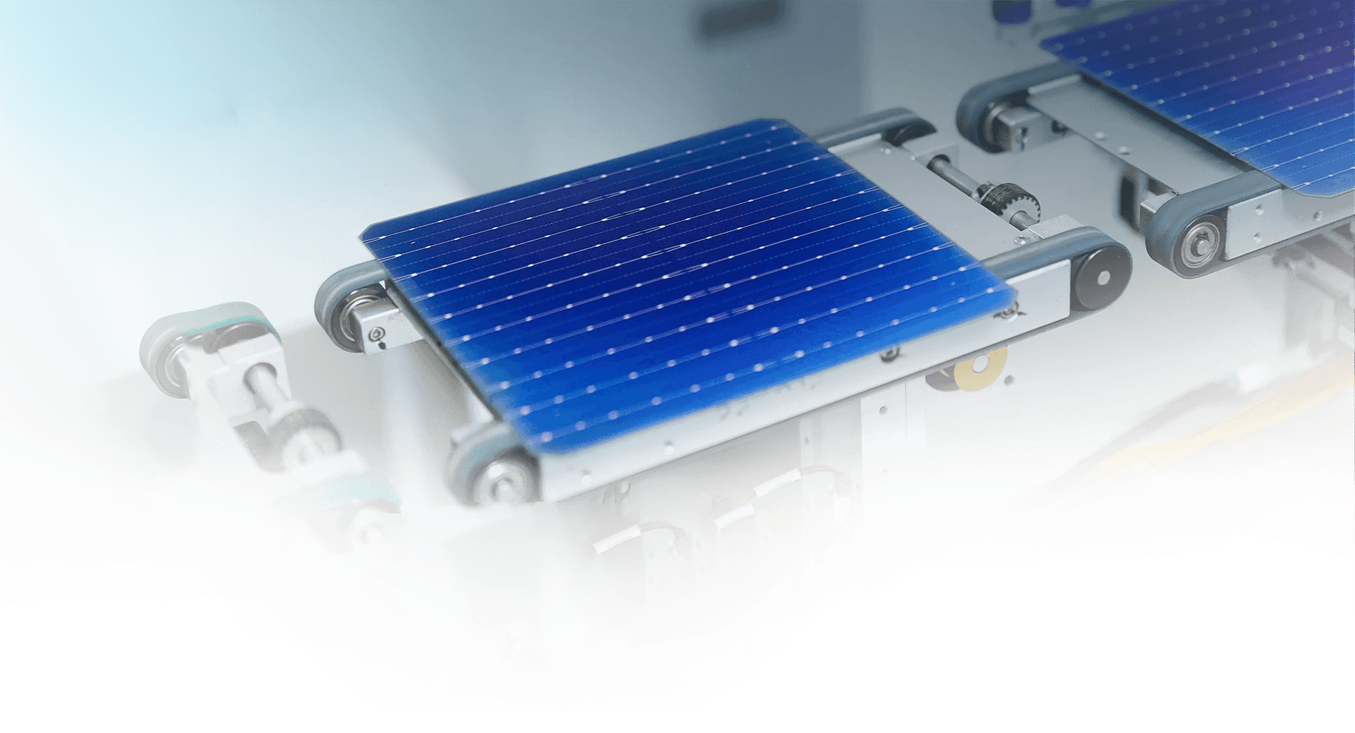
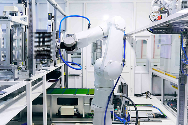
Our facilities in Baddi, Himachal Pradesh embody solar cell production. Backed by 16 years of experience and compliance to quality, safety, and environmental standards, we deliver high-efficiency cells. Our cleanroom, coupled with lean operations, ensures project execution and cost-effectiveness. With a focus on innovation and future-ready technology, we are committed to industry leadership.
800
MW
Ramp Up
Under Process
1
GW
Plant Certifications
by TUV RhienlandProducts Certifications
by
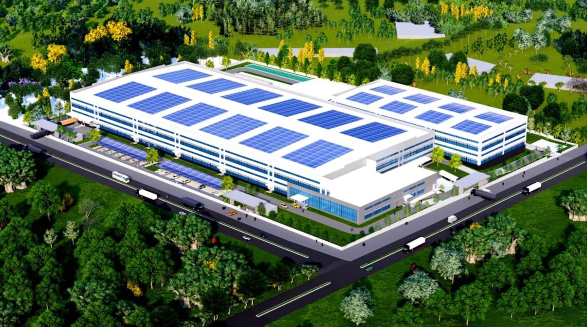
Manufacturing Units in Bhubaneswar, Odisha
We are in advanced stages of establishing cutting-edge integrated solar cell and solar module manufacturing facilities in Bhubaneswar, Odisha. With commissioning planned in 2025, the facilities will have a cumulative solar cell and solar module production capacity of 4 GW and 2.8 GW respectively. One of the upcoming units is a Joint Venture with a prominent renewable energy service provider in India. Leveraging on our technological and operational excellence, we are committed to adopting latest technologies and meeting execution timelines to drive sustainable growth while supporting global clean energy goals.